
Let's take a look at what a typical DDR2 memory module may look like:
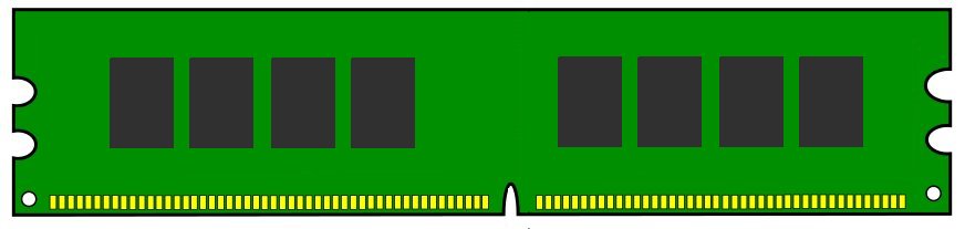
In the picture above one can see a module with 8 grey memory ICs (integrated circuits). These ICs are the memory chips and a module (as in a stick of memory) can hold a number of such chips, situated on either a single or both sides, which are connected together in order to provided the rated memory capacity of the module.
For example, let's assume the above module is a 512 MB module and that there are 8 memory chips situated only on a single side of the module (as pictured).
Each side of the module is called a rank, so in our example, the module is considered to be single ranked (as there are no chips on the other side).
In order for us to get the 512 MB capacity, each chip needs to hold 64MB of data (as capacity = ranks x chips x chip_capacity, therefore chip_capacity = 512 MB / (1 rank x 8 chips) = 64 MB).
In our example, we will assume that this 512 MB module is the only module in our system. The module is plugged in to the motherboard into what's known as a channel. If we had more than this single module in our system, each module would be connected to it's own channel.
We now know that the memory capacity of a system is made up of a number of memory modules situated in a respective number of channels; each memory module made up of 1 or 2 ranks of memory IC (integrated circuit) chips, each IC able to store a certain amount of data.
It's time to zoom in further and take a look at the individual memory ICs (chips) that actually store the data.
The memory chips are actually matrices of transistors that store the bits of memory. I'm not going to go into the operation of DRAM here; that's another topic and there's plenty been written about that if you're interested. We are rather going to focus on how these 'bits' of memory are laid out in the IC.
Targetting these individual bits further, as mentioned, they are laid out in a matrix. This matrix, or 'grid', is made up of a number of rows and columns where each row-column pair points to 8 bits (1 byte) of memory. In fact, in each of these ICs, there are up to 4 'sets' of matrices (in DDR2). Each one of these 'sets'; is called a bank. This physically may be laid out something like the below:
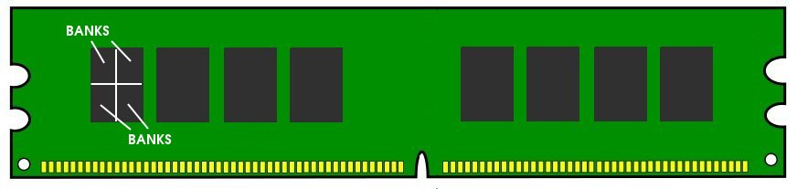
So to recap, in our example, we have 1 channel of memory, made up of 1 rank of 8 chips. Each such IC has 4 banks of memory. Each bank made up of rows x columns bytes.
Now doing the math:
512 MB = 1 channel x 1 rank x 8 chips x 4 banks-per-chip
Therefore, each bank = 16 MB.
So how many rows and columns are there in each bank? Well this will be specified on the datasheet for the memory chip. However there can only be a maximum of 16,384 (16K) rows on a DDR2 module. This is due to there only being 14 address lines (A0-A13).
So in our example, let's assume we've got the maximum number of rows (16K, or 14 bits). In order to make up the 16 MB per bank, there must be 1,048 (1K), or 10 bits, of columns (16K * 1K = 16MB).
The final tally is therefore as follows:
512 MB = 1 channel * 1 rank * 8 chips * 4 banks * 16K rows * 1K columns
Now that we've got our example, let's take a look at how these bytes are addressed.
The first thing one should understand is that when we speak about 'physical' memory addresses, these addresses don't directly map 1-1 with the address lines on a memory module. Rather these 'physical addresses' are representitive of the actual location of data stored on the actual memory module(s). What I mean by this is that from looking at any particular physical address, say 0xf0000000, without knowing anything else about the system, it is difficult for one to know with any particular certainty which actual physical memory 'chip' - and, importantly - where on the chip any data written to this address will physically be stored. In order to work that out, it's useful to understand what the memory controller is doing in order to store our data.
When the CPU transacts data from memory, the memory controller is responsible for fulfilling that request. It takes the physcial memory address passed to it by the CPU and addresses the relevant location in the physcial memory module. This process looks something like the following:
CPU: Hey memory controller, go fetch me the byte at 0x10001fd8
MEM_CONTROLLER: Hey memory module in Channel 0, give me the bytes from Rank 0, Bank 0, Row 8192, Column 1019
You'll notice in the example that the memory controller didn't request a byte from any specific memory chip on the module, rather it requested the byte stored in Bank 0, Row 8192, Column 1019 from all ICs on Rank 0 on the chip! This means that instead of receiving just 1 byte, it would have received 8 bytes (from the 8 ICs). This is in fact always the case for DDR2 memory. Any memory access will always return 64-bit (8 bytes) of data.
Wait a minute! Every time a single byte is requested, a full 8 bytes are returned??
Well yes; there is no way to address a specific IC. In fact the fact that 8 bytes are returned is actually advantageous and saves multiple lookups in many cases (as when accessing congruent memory addresses).
We can use the following analogy to hopefully make things slightly clearer.
Imagine 8 identical buildings lined up side-by-side. In each building you have 4 wings, multiple floors and on each floor a certain number of apartments. Each apartment holds exactly 8 people.
Now in order to get a certain person to exit a building you need to shout up and tell everyone who it is that you wish to exit. So you might shout out something like: Can the person in building 5, east wing, floor 10, apartment 1, standing 3rd from the left in the apartment please come out!.
Now imagine that you had no way to specify exactly which person in the apartment should come out. You'd have to call out Can the people in building 5, east wing, floor 10, apartment 1 please come out!. All 8 people in that apartment would then come out and you'd have to chose the person you wanted from those 8.
Now let's take this one step further. You have now lost the ability to specify which building the person is situated in. You'd have to ask Can all the people in the east wing, floor 10, apartment 1 please come out!. Now you 64 people in those apartments across all the buildings would come out (8 from each building).
This is exactly what the memory controller is doing. It is only able to address the row (floor) and the column (apartment) in each bank (wing) across all the chips (buildings) for each rank (group of buildings). As mentioned, each location holds 8 bits (the 8 people) and such a request would therefore transact all 64 bits - 8 bytes of data.
So how does the memory controller know which one of these 8 bytes has been addressed in the request?
It uses the 3 least significant bits of the physical address as an index to choose the relevant byte. Remember when we said that the 'physical' address isn't sent over-the-wire directly to the actual memory? This is a perfect example of this; these 3 bits of the address are never sent to the actual chips at all!
So if we take a look at the following addresses, we can see that each one will effect the exact request by the memory controller to the actual RAM:
'physical' address    actual memory address
0x00f00010            ->  0x00f00010
0x00f00011            ->  0x00f00010
0x00f00012            ->  0x00f00010
0x00f00013            ->  0x00f00010
0x00f00014            ->  0x00f00010
0x00f00015            ->  0x00f00010
0x00f00016            ->  0x00f00010
0x00f00017            ->  0x00f00010
And we can see why this is an advantageous optimization. Memory is often accessed sequentially in allocated chunks. Reading 8 bytes from an aligned buffer would only require a single access of RAM. The 8 bytes accessed are stored in a line cache so each byte read subsequent to the first one would simply read it straight from this line cache without requesting further from physical memory. When such a buffer is written, it can too be written in 8-byte blocks. Furthermore, it will be 'spread' over all the 8 ICs on the rank meaning that the ICs would be loaded uniformly and there would be no single IC being worn out unnecessarily.
Let's recap. We now know that DDR2 memory is accessed 8 bytes at a time. It is addressed by specifying the channel (which memory module to use), the rank (which side of the memory module), the bank (which one of the up-to-4 parts of the actual memory chips), the row and the column. Once all 8 bytes are read into the line cache, the controller can use the last 3 bits of the physical address to index the correct byte in the line.
Now let's take a look at the other (non 3 least significant) bits of the physical address and see how they relate to the addressing.
As it turns out, the specific details of this differ across different chipset generations. For example, Sandy Bridge chipsets will map certain bits of the physical address to certain locations in actual memory whilst the very next generation, Ivy Bridge will perform the mapping slightly differently. As Intel doesn't publically document this mapping, they need to be reverse engineered. You can see Mark Seaborn's post where he discusses his mapping on Sandy Bridge for his particular RAM configuration and the Reverse Engineering Intel DRAM Addressing and Exploitation paper where they present a few methods for discerning these mappings for any arbitrary RAM configuration on an arbitrary chipset generation.
To reverse engineer the addresing scheme for a Core 2 Duo system (old I know), I used a low-bandwidth physical instrumentation method (which I'll detail in a subsequent post; stay tuned!).
To further our discussion, I'm going to describe the mappings for our example of a single channel of single-ranked DDR2 memory made up of ICs of 4 banks, 16K rows and 1K columns each on a Core 2 Duo system:
Bit
0..2      byte-index into 8-byte cache line
3..12     column address (A0-A9)
13.14     bank*
15        row address (A11)
16..26    row address (A0-A10)
27..28    row address (A12-A13)
* Bank is selected by XORing row bits 18,19 with bits 13,14 respectively
Using these mappings we can now work out exactly where the data will physically be located on the actual physical memory chips. For example, the address 0x10001fd8 or 0b00010000000000000001111111011000 would be situated as follows:
00  01000000000000  00  1111111011  000
          |         |        |       |
          |         |        |        -- index 0
          |         |         -- column 1019
          |          -- bank 0 (XORed with row bits)
           -- row 8192
Keep in mind that if we had more than a single rank and another memory module or two (i.e. some additonal channels), we would need bits in the address to specify which rank + module to target and therefore the mapping described above would be slightly different.
In a subsequent post, I'll be diving deeper into how RAM is accessed by the memory controller (what gets sent over the bus) and will detail how I reverse engineered the above scheme.